ADVERTISE WITH USReach Embedded Science readers →
GaN-on-Silicon Moves to 300-mm Wafers as imec Targets Lower-Cost Power Devices
Imec is developing 300-mm GaN-on-silicon power devices with industry partners to improve manufacturing economics and enable advanced devices.
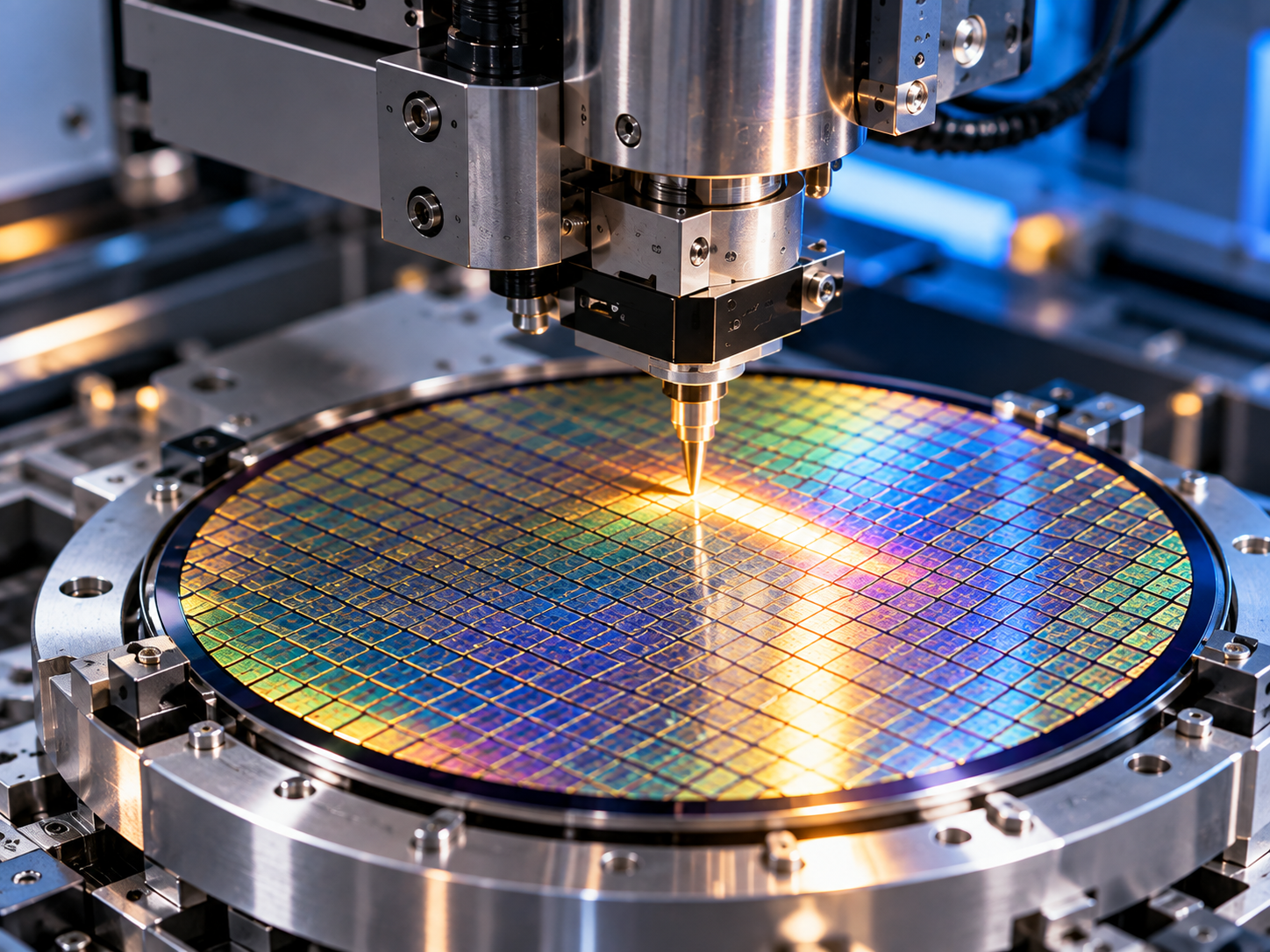
Imec is moving gallium-nitride power semiconductor development onto 300-mm wafers, opening a potential path toward lower manufacturing costs and more advanced GaN devices using infrastructure developed for the silicon semiconductor industry. The research organization launched its 300-mm GaN program with AIXTRON, GlobalFoundries, KLA, Synopsys and Veeco as initial partners. The program begins with low-voltage p-GaN HEMTs fabricated using 300-mm silicon substrates, with higher-voltage devices to follow.
Key Points
- Imec is developing GaN power devices on 300-mm wafers after years of work on 200-mm GaN-on-silicon technology.
- Initial development uses 300-mm Si(111) substrates for p-GaN HEMTs at 100 V and above, with 650-V-and-higher development planned on engineered substrates.
- The move to 300 mm is intended to reduce manufacturing cost while giving GaN development access to advanced CMOS fabrication equipment.
GaN Is Moving Into Silicon’s Manufacturing World
Gallium nitride has already become an established alternative to conventional silicon in applications where high-frequency switching, efficiency and power density are especially important. What is changing is how GaN is manufactured. Most current high-volume GaN power production uses wafer sizes smaller than the 300-mm format common in advanced silicon manufacturing. Imec says GaN manufacturing capacity is now largely available at 200 mm.
A 300-mm production environment provides access to equipment, process controls, automation and manufacturing techniques developed through decades of silicon CMOS scaling. That could matter as GaN moves beyond discrete power switches toward integrated power devices.
Starting With GaN on 300-mm Silicon
Imec’s initial platform uses 300-mm Si(111) silicon wafers. The organization is developing a baseline lateral p-GaN high-electron-mobility transistor (HEMT) technology platform for applications beginning around 100 V. Development includes p-GaN etching and formation of low-resistance ohmic contacts.
Access to advanced 300-mm equipment may allow more aggressively scaled low-voltage p-GaN gate HEMTs for point-of-load conversion near CPUs and GPUs, where efficient power conversion in limited space is increasingly important.
The Economics of a Larger Wafer
More devices can be fabricated during one processing cycle on a larger wafer. A 300-mm wafer has substantially more surface area than a 200-mm wafer, but that does not automatically make each chip cheaper. Yield, epitaxial growth, wafer bow, defect density, process complexity and capital utilization affect the economics. Imec identifies cost reduction as an explicit goal of its program.
650 V and Higher Present a Different Challenge
For devices at 650 V and above, imec plans 300-mm engineered substrates with a polycrystalline aluminum-nitride core. Higher-voltage epitaxial layers increase mechanical stress, making wafer bow and mechanical strength important process-development challenges at 300 mm.
An Entire Manufacturing Ecosystem Is Involved
AIXTRON contributes epitaxial-growth equipment; GlobalFoundries, large-scale manufacturing expertise; KLA, process control and inspection; Synopsys, electronic design automation; and Veeco, semiconductor processing technology. Imec provides the common research-and-development platform. Wafer materials, metrology, design tools, packaging, reliability testing and production-scale controls all need to mature together.
TI Shows 300-mm GaN Is Moving Beyond Research
Texas Instruments has also reported 300-mm GaN-on-silicon manufacturing development and customer samples using its proprietary process. TI reports more than 80 million device-hours of reliability testing across its GaN technology. Imec’s program differs in its multi-company industrial research structure.
GaN May Exploit Silicon Rather Than Replace It
GaN is often described as a replacement for silicon in power electronics. The manufacturing trend is more nuanced: GaN transistors can provide switching advantages while leveraging silicon substrates and the established CMOS manufacturing ecosystem. That combination could make advanced GaN devices more practical economically.
Development Status
Imec launched its 300-mm GaN power-electronics program in October 2025, with installation of full 300-mm capabilities targeted for the end of that year and development continuing through 2026. The platform remains an R&D and industrial-development program rather than a packaged retail semiconductor product. Imec’s broader GaN research covers device concepts from approximately 40 V to 1200 V.
Price, Purchasing and Availability
There is no public unit price, distributor inventory or conventional purchasing link for imec’s 300-mm GaN research platform. Companies can pursue participation through imec’s GaN Industrial Affiliation Program and related research partnerships.
First-Party Source Material and Further Reading
Imec: 300-mm GaN Program; GaN Power Devices and 200-mm/300-mm Technology; and Advancing GaN Power Technologies: Scaling to 300 mm for the AI Era. Texas Instruments provides additional first-party information about its own 300-mm GaN-on-silicon development and customer sampling.
Original announcement: imec, Imec launches 300mm GaN program to develop advanced power devices and reduce manufacturing costs, October 6, 2025. Imec is based in Leuven, Belgium; commercial participation is through research partnerships and technology licensing.