ADVERTISE WITH USReach Embedded Science readers →
Making Photonic Chips Survive Extreme Environments
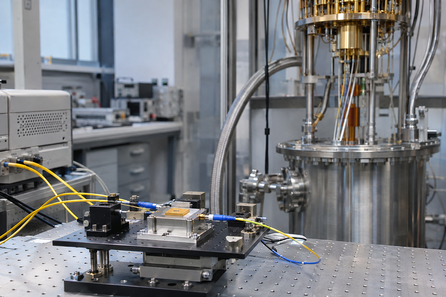
A photonic chip needs reliable connections to the equipment around it. NIST researchers are developing packaging that maintains those connections through demanding environmental conditions.
A photonic chip needs reliable connections to the equipment around it. NIST researchers are developing packaging that maintains those connections through demanding environmental conditions.
- Fiber alignment is essential to useful optical performance.
- An inorganic bonding method replaces a vulnerable adhesive connection.
- Environmental testing must distinguish complete assemblies from material samples.
The Connection Can Determine Whether a Chip Works
A photonic integrated circuit guides light through microscopic structures. To become part of an instrument, it must transfer that light reliably between the chip and external optical fibers.
That connection is a mechanical problem as well as an optical one. Movement can alter alignment, while changes in temperature or exposure conditions can damage the materials holding the assembly together.
An excellent optical circuit therefore needs packaging that preserves its operating geometry. For instruments intended for unusual environments, packaging becomes part of the core technology.
Replacing an Organic Adhesive
NIST adapted hydroxide-catalysis bonding to attach optical fibers to photonic chips. The process forms an inorganic, glasslike chemical connection using a small quantity of sodium hydroxide solution.
The researchers demonstrated a fiber connection that remained intact through cryogenic conditions, temperature changes, radiation exposure, and high vacuum. NIST identifies the method as a route toward more resilient photonic instruments.
The underlying bonding approach has a history in precision optics. LIGO’s engineering documentation, for example, describes silicate bonding procedures and the importance of surface contact and cleanliness.
Adapting a process to photonic packaging requires maintaining the precise alignment needed for light coupling, rather than simply demonstrating a strong mechanical joint.
What the Tests Establish
The reported environmental tests support the resilience of the demonstrated assembly under specified conditions.
High-temperature performance needs more careful wording. NIST states that limitations of the available commercial optical fibers prevented direct high-temperature testing of the complete packaged photonic chip. Additional studies supported the mechanical stability of the bonding method at higher temperatures.
The research paper also identifies fiber coatings and other package components as factors that can limit operation in extreme heat.
A package is a collection of materials. Improving one connection does not automatically extend every other component’s operating range.
From a Resilient Bond to a Manufactured Product
The present bonding process takes several days. NIST describes shortening that process as an engineering development task.
Manufacturing would also require repeatable alignment, predictable bond quality, and a way to inspect assemblies efficiently. These requirements influence how many usable devices a process produces.
For a particular mission, qualification would need to match the actual exposure: temperature history, radiation conditions, vacuum requirements, and mechanical loading. The demonstrated process provides evidence for that work without establishing universal suitability for every harsh environment.
Sources: NIST’s packaging announcement; research paper; LIGO bonding procedure.
Explore Embedded Science or purchase a membership. Purchases do not automatically renew.