ADVERTISE WITH USReach Embedded Science readers →
Flexible Transparent Photonic Chips Move Toward Manufacturing
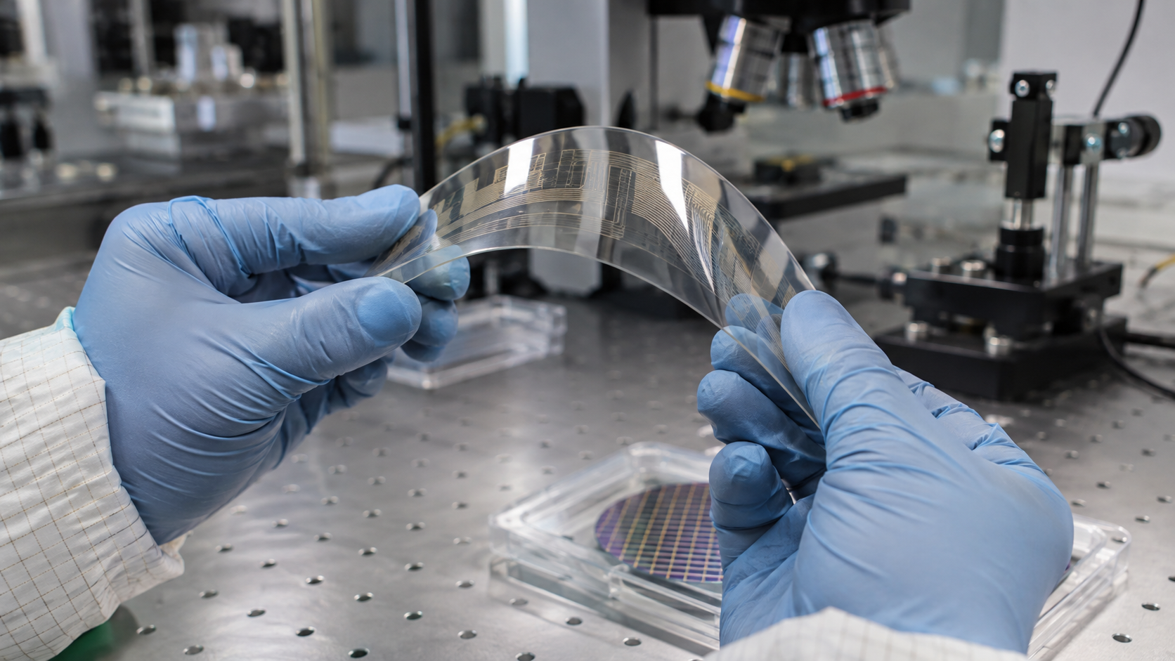
MIT researchers and NY Creates engineers have developed a wafer-scale process for flexible, transparent photonic chips. The work connects optical functionality with a manufacturing approach intended to produce more than isolated laboratory devices.
MIT researchers and NY Creates engineers have developed a wafer-scale process for flexible, transparent photonic chips. The work connects optical functionality with a manufacturing approach intended to produce more than isolated laboratory devices.
- The process begins with established semiconductor fabrication methods.
- Temporary supports allow most of the rigid substrate to be removed.
- Optical performance, transparency, and repeated bending require separate tests.
Giving Integrated Optics a Different Physical Form
Integrated photonics puts optical functions into compact manufactured structures. Many applications, however, would benefit from surfaces that bend or allow visible light to pass through.
Those properties introduce additional requirements. The optical circuit must continue working while its supporting structure changes shape, and transparency must be assessed for the intended use.
A curved display element, for example, needs both optical functionality and a suitable physical form. Fabricating a few successful samples is an early step; producing them across a wafer raises questions about uniformity and process control.
Removing the Rigid Support
MIT’s September 2026 announcement describes a fabrication platform using 300-millimeter wafers.
The process first creates optical structures using a rigid wafer. A temporary supporting wafer is attached, allowing the original substrate to be removed while preserving the thin functional layers. A transparent polyester film then supports the remaining structure.
The researchers managed fabrication stress and used a combination of thinning and selective removal processes to protect the optical layers.
The sequence matters. A layer that is strong enough when supported by a thick wafer may be difficult to handle on its own. Temporary supports make it possible to perform intermediate manufacturing operations without requiring the final flexible structure to carry every load.
Testing More Than Bendability
MIT reports repeated bending tests without a drop in performance under the tested conditions. The team also assessed the optical behavior of waveguides and the transparency of the resulting platform.
Those measurements address different questions. A sheet can bend successfully while transmitting light poorly. Conversely, a transparent material may still scatter light or create visual distortion that matters in a display application.
The work appears in Optica, with a related account in MIT’s 2026 microsystems research report.
What Manufacturing Readiness Would Add
A production assessment would examine the distribution of performance across wafers and manufacturing runs. It would also establish acceptable bending conditions and the effects of repeated handling.
Packaging remains relevant. Flexible chips still require connections, protection, and a way to become part of a usable product.
The demonstrated platform addresses a manufacturing pathway for flexible, transparent photonics. Application-specific durability, assembly, and lifetime testing would determine how that platform performs in a particular wearable, display, or sensing system.
Sources: MIT’s research announcement; Optica publication; MIT’s 2026 research report.
Explore Embedded Science or support independent reporting. Purchases do not automatically renew.