ADVERTISE WITH USReach Embedded Science readers →
GaN Isn’t Replacing Silicon: ST Is Building AI Power Systems With Si, SiC and GaN
GaN Isn’t Replacing Silicon: ST Is Building AI Power Systems With Si, SiC and GaN
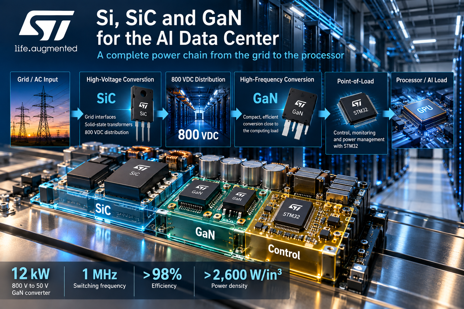
STMicroelectronics is developing next-generation AI data-center infrastructure around a combination of silicon, silicon carbide and gallium nitride rather than betting on a single semiconductor technology. Its emerging 800-VDC architecture uses SiC for demanding high-voltage conversion, GaN for compact high-frequency conversion closer to processors, and silicon-based controllers and supporting electronics throughout the power chain. ST has already demonstrated a 12-kW GaN converter operating from an 800-V input at 1 MHz with more than 98% efficiency. The architecture illustrates an important semiconductor trend: GaN and SiC increasingly complement silicon rather than simply replacing it.
Key points
- ST’s AI power strategy combines silicon, SiC and GaN, assigning each semiconductor technology to power-conversion stages where its characteristics offer an advantage.
- ST has demonstrated a 12-kW, 800-V-to-50-V GaN converter operating at 1 MHz with more than 98% efficiency and power density exceeding 2,600 W/in³.
- The larger development is a transition toward heterogeneous power electronics, where semiconductor material is selected according to voltage, frequency, efficiency, thermal and cost requirements rather than using one technology throughout the system.
AI Is Creating a Power Problem
Artificial intelligence is changing more than processors and software.
The enormous electrical requirements of high-density GPU clusters are forcing engineers to reconsider how power enters a data center, travels through a rack and ultimately reaches the processor.
Traditional data-center architectures commonly distribute power at much lower voltages. That becomes increasingly problematic as rack power rises from kilowatts toward hundreds of kilowatts and potentially megawatts.
Moving enormous amounts of power at relatively low voltage requires correspondingly high current.
High current means larger conductors, greater resistive losses, more copper and increasingly difficult thermal management.
STMicroelectronics says next-generation AI infrastructure is therefore moving toward high-voltage DC distribution, with 800 VDC emerging as an important architecture for future high-density computing.
Instead of repeatedly converting electricity through numerous intermediate stages, 800-VDC architectures can distribute higher-voltage power through the rack before converting it nearer the computing load.
The change creates an interesting semiconductor engineering problem.
No single semiconductor technology is necessarily ideal for every stage.
SiC Handles the High-Voltage Front End
ST positions silicon carbide primarily toward the high-voltage side of its AI infrastructure.
That includes grid interfaces, solid-state transformers and high-voltage DC distribution.
SiC is a wide-bandgap semiconductor with characteristics that make it particularly useful where high voltage, high power and efficiency are required.
ST currently manufactures SiC devices spanning voltage classes from approximately 650 V through 1700 V.
At these higher-voltage stages, switching frequency is not the only consideration. Engineers must balance conduction losses, switching losses, voltage capability, thermal behavior, reliability and cost.
ST therefore uses SiC where its high-voltage capabilities provide an advantage.
But moving closer to the processors changes the engineering requirements.
That is where GaN becomes increasingly interesting.
GaN Moves Closer to the Processor
Gallium nitride offers very different characteristics.
Its high electron mobility, low capacitance, low gate charge and ability to switch extremely rapidly make GaN particularly attractive for high-frequency power conversion.
Higher switching frequencies can allow engineers to reduce the size of transformers, inductors and other passive components.
That can produce smaller and considerably more power-dense converters.
ST consequently positions GaN closer to the computing load, where electrical power must be converted efficiently inside extremely constrained spaces.
The company has now demonstrated what this approach can accomplish.
Its prototype AI data-center power-delivery board converts an 800-VDC input directly to 50 V.
The converter delivers 12 kW continuously.
It operates at a switching frequency of 1 MHz.
ST reports efficiency above 98% and power density exceeding 2,600 W/in³.
The complete power board is approximately the size of a smartphone.
Those numbers represent ST’s prototype system performance rather than universal specifications for GaN converters, but they demonstrate why high-frequency wide-bandgap semiconductors are attracting so much attention in high-density computing.
Inside ST’s 12-kW Converter
ST’s technical documentation provides a particularly useful look inside the system.
On the primary side, the converter uses high-voltage GaN drivers and 650-V GaN power transistors.
The conversion stage feeds a matrix transformer before reaching the secondary side.
There, ST uses 100-V GaN power transistors and low-voltage GaN drivers.
Control is provided by an STM32G474 microcontroller.
That device uses an Arm Cortex-M4 core and provides the high-resolution timing capabilities needed to control the high-frequency power-conversion system.
The architecture is therefore not simply a “GaN power supply.”
It combines high-voltage GaN, low-voltage GaN, conventional silicon control electronics, gate drivers, magnetics and other semiconductor components into one coordinated power system.
That distinction is important.
Silicon Hasn’t Gone Away
Much of the discussion surrounding wide-bandgap semiconductors has centered on whether GaN or SiC will replace conventional silicon.
ST’s architecture illustrates why that question can be misleading.
Silicon remains deeply embedded in the system.
Microcontrollers, analog devices, mixed-signal circuits, sensing components, power-management ICs, drivers and other silicon devices perform essential control and monitoring functions.
ST’s current AI server power portfolio includes STM32 digital controllers, analog and sensing devices, isolated gate drivers, DC-DC converters, protection devices and conventional power MOSFET technologies alongside GaN and SiC.
Even individual power stages can combine technologies.
ST’s 800-V-to-50-V development platform includes GaN power transistors controlled by silicon-based electronics.
Rather than disappearing, silicon increasingly acts as the intelligence and control infrastructure surrounding wide-bandgap power devices.
The Semiconductor Depends on the Job
The result is a more nuanced power architecture.
At the high-voltage front end, SiC can provide the voltage capability and efficiency required to handle large amounts of power.
Closer to the processors, GaN’s extremely fast switching can increase converter power density and reduce the size of passive components.
At lower voltages and within the control architecture, mature silicon technologies remain highly useful.
The engineering decision therefore becomes less about choosing a winning semiconductor material and more about selecting the appropriate material for each stage.
ST summarizes its own data-center strategy as covering the complete power chain using SiC, GaN, low-voltage devices and control systems.
That approach could become increasingly common as power systems become more demanding.
Why 800 VDC Changes the Equation
The move toward 800-VDC rack distribution is a major reason this heterogeneous semiconductor architecture is becoming relevant.
Today’s approximately 54-V distribution systems were developed for much lower rack power.
At megawatt scale, transmitting the same amount of power at 54 V requires enormous current.
An idealized 1-MW load at 54 V would require roughly 18,500 A before conversion losses are considered.
At 800 V, the equivalent calculation is approximately 1,250 A.
Actual data-center architectures are considerably more complicated than that simple calculation, but it demonstrates the electrical reason engineers want to increase distribution voltage.
Higher voltage dramatically reduces the current required to transmit a given amount of power.
That can reduce conductor size, copper requirements and resistive losses.
But higher voltage also creates greater demands on switching devices.
That gives high-voltage SiC and GaN devices an increasingly important role.
From 800 V Down to the GPU
The final processor does not operate anywhere near 800 V.
Power therefore still has to travel through several conversion stages before reaching a GPU, CPU or accelerator core.
ST describes the path broadly as:
Grid → high-voltage conversion → 800 VDC distribution → rack conversion → intermediate voltage → processor voltage
Its current development work includes 800-V-to-50-V conversion as well as newer architectures converting 800 V directly to 12 V and 6 V.
ST says eliminating intermediate conversion stages can reduce system losses, copper usage and infrastructure complexity.
The company is developing these architectures in collaboration with NVIDIA for future AI data-center reference designs.
The objective is ultimately to place more computing power within a rack without allowing electrical conversion equipment and cooling infrastructure to consume an unacceptable portion of the available space and energy.
More Than Power Semiconductors
ST’s Cloud AI strategy extends beyond the power chain.
The company is also developing silicon photonics, BiCMOS electronics, mixed-signal devices and STM32 microcontrollers for data-center infrastructure.
Silicon photonics addresses another increasingly important AI problem: moving enormous quantities of data between processors.
As electrical copper connections become increasingly difficult to scale in bandwidth and energy consumption, optical communication is moving progressively closer to the computing hardware.
ST’s larger architecture therefore combines two trends occurring simultaneously.
Wide-bandgap semiconductors are changing how electrical power moves toward the processor.
Silicon photonics is changing how information moves between processors.
Conventional silicon electronics provide control and interface functions connecting those systems.
Manufacturing Has Become Part of the Strategy
ST is also investing in the manufacturing infrastructure needed to support these technologies.
The company says its Italian operations provide high-volume 200-mm silicon-carbide production for high-voltage power conversion.
Its French 300-mm fabs manufacture digital, mixed-signal and silicon-photonics technologies.
ST is also expanding SiC manufacturing through its joint venture with Sanan Optoelectronics in China.
This matters because widespread adoption of SiC and GaN ultimately depends on more than laboratory performance.
Manufacturing capacity, wafer size, yield, packaging, reliability and cost will determine where these technologies can economically replace or supplement silicon.
GaN Versus Silicon May Be the Wrong Question
ST’s AI infrastructure work provides a useful counterpoint to the idea that semiconductor development is simply a competition among silicon, GaN and SiC.
All three can coexist within the same power system.
The more meaningful question is where each technology provides sufficient electrical or system-level advantages to justify its use.
SiC can dominate one conversion stage.
GaN can dominate another.
Silicon can control both.
That model could extend well beyond AI data centers into electric vehicles, renewable-energy systems, industrial power supplies, battery storage and other applications requiring increasingly sophisticated power conversion.
The semiconductor industry’s next stage may therefore be less about replacing silicon than combining materials intelligently.
For engineers, that means the future of power electronics may not belong to one semiconductor.
It may belong to systems capable of using several.
Development Status
ST’s 800-VDC technology is under active development for next-generation AI infrastructure.
The company demonstrated its 12-kW, 800-V-to-50-V GaN converter in 2025 and provided additional technical details at APEC 2026.
ST has since expanded the architecture with direct 800-V-to-12-V and 800-V-to-6-V development platforms.
The company is working with NVIDIA on architectures aligned with NVIDIA’s next-generation 800-VDC AI data-center infrastructure.
ST also maintains an established commercial portfolio of SiC MOSFETs, GaN transistors, silicon power devices, STM32 microcontrollers, gate drivers and associated power-management products.
The complete 12-kW AI power-delivery architecture should therefore be distinguished from an individual production component. It is currently a development and reference architecture incorporating multiple ST technologies.
Price, Purchasing and Availability
There is no published retail price for ST’s complete 12-kW, 800-VDC AI power-delivery system.
It is a development platform rather than a conventional off-the-shelf power supply.
Many of the semiconductor components underlying the architecture are commercially available individually through ST and its authorized distributors.
ST’s APEC 2026 documentation identifies components including the SGT023R70FTP 700-V GaN transistor, SGT1D5R10MEA 100-V GaN transistor, STGAP2G isolated GaN gate driver, STPRDC02 GaN and silicon driver, and STM32G474 microcontroller.
Pricing and availability depend on the specific component, quantity and distributor.
First-Party Source Material
STMicroelectronics — STMicroelectronics and the Infrastructure of Cloud AI
This is the primary ST article and provides the broader architecture behind the story, including SiC, GaN, silicon, silicon photonics, BiCMOS and STM32 technologies across the AI data-center infrastructure.
STMicroelectronics — 800 VDC Power Solutions for Next-Generation AI Factories
ST’s October 2025 announcement details its 800-VDC development program and specifically describes the combination of silicon carbide, gallium nitride and silicon technologies. It also documents the 12-kW GaN converter operating from an 800-V input at 1 MHz, with greater than 98% efficiency and power density exceeding 2,600 W/in³.
STMicroelectronics — High-Density Power Delivery Solutions for Next-Generation AI Data Centers
This ST technical white paper examines why traditional 54-V data-center power architectures are becoming increasingly difficult to scale and describes ST’s 800-V-to-50-V approach. The design centers on a 12-kW, 1-MHz GaN LLC resonant converter developed for next-generation AI infrastructure.
STMicroelectronics — 12 kW HVDC Converter: 800 V to 50 V, APEC 2026
This is particularly useful for engineers because ST identifies the actual components inside the prototype. The architecture includes 700-V and 100-V GaN power transistors, GaN gate drivers, a matrix transformer and an STM32G474 digital-power MCU.
STMicroelectronics — PowerGaN Technology and Products
ST’s PowerGaN technical resource explains the electrical advantages behind the technology, including low on-resistance, low gate charge, negligible or zero reverse-recovery charge, low intrinsic capacitances and high-frequency switching capability.
STMicroelectronics — PowerGaN Technical Documentation
This is ST’s technical-document library for its PowerGaN portfolio. It includes datasheets, application notes, driving guidance, device-robustness information and product presentations covering ST’s GaN power devices.
STMicroelectronics — 100 V PowerGaN for AI Servers and High-Current Power Conversion
This provides additional first-party information on ST’s low-voltage GaN strategy. ST explains how ultralow RDS(on), low gate charge, zero reverse recovery and fast switching are being used for compact, high-current conversion in AI servers and other power-dense systems.
Further Reading
ST’s High-Density Power Delivery Solutions for Next-Generation AI Data Centers is the strongest engineering companion to the original article. It examines the transition from traditional 54-V architectures toward 800-V distribution and describes the company’s 12-kW, 1-MHz GaN LLC resonant converter developed around an 800-V-to-50-V conversion stage.
The 12 kW HVDC Converter: 800 V to 50 V — APEC 2026 technical document goes further by identifying individual semiconductor components within the converter. These include the SGT023R70FTP high-voltage GaN transistor, SGT1D5R10MEA 100-V GaN transistor, STGAP2G isolated GaN gate driver, STPRDC02GN GaN/silicon driver and STM32G474 digital-power microcontroller.
ST’s PowerGaN Technology material provides useful background on why GaN is attractive for high-frequency conversion. ST highlights characteristics including low gate charge, low intrinsic capacitance, zero or negligible reverse-recovery charge and operation at much higher switching frequencies, allowing engineers to reduce system size while increasing power density.
For an additional look at the 800-VDC development program, ST’s 800-V HVDC AI Data Center technical article documents the development of its 6-kW, 12-kW and 20-kW power-delivery boards and provides background on the NVIDIA collaboration and the evolution of the prototype.
Original Article
STMicroelectronics — “STMicroelectronics and the Infrastructure of Cloud AI”
Published June 26, 2026.
Read the Original STMicroelectronics Article
The article places ST’s power-semiconductor development within a larger Cloud AI strategy. ST describes a grid-to-core architecture incorporating SiC and GaN power devices, 800-VDC distribution, silicon photonics, BiCMOS electronics, mixed-signal devices and STM32 control.
Contact and Purchasing
STMicroelectronics
Geneva, Switzerland
ST provides purchasing, samples, evaluation hardware, development resources and authorized-distributor availability through its individual product pages.
STMicroelectronics — PowerGaN Product Portfolio
The PowerGaN page provides access to individual GaN transistor product pages, specifications, documentation and product-selection resources.
STMicroelectronics — PowerGaN Documentation
This resource provides datasheets and engineering documentation for ST’s commercially available PowerGaN devices.
STMicroelectronics — 100 V PowerGaN Products
ST provides direct “Order now” access for devices including its SGT1D5R10MEA 100-V, 1.1-mΩ PowerGaN transistor used for high-current power-conversion applications.
Complete 12-kW 800-VDC system price: Not publicly listed
Complete 12-kW system availability: Development/reference architecture rather than a conventional retail power supply
Individual semiconductor availability: Product dependent
Commercial components: Available through STMicroelectronics and its authorized distribution network
Development resources: Datasheets, application notes, evaluation hardware, reference designs and engineering documentation are available through ST’s individual product and technology pages.